Transistors and memory get together
NRL's "0.5T0.5R" - 2D materials based hybrid memory cell that changed RRAM technology history and revolutionized in-memory computing is highlighted by Nature Electronics.
Excerpt from Nature Electronics by Stuart Thomas
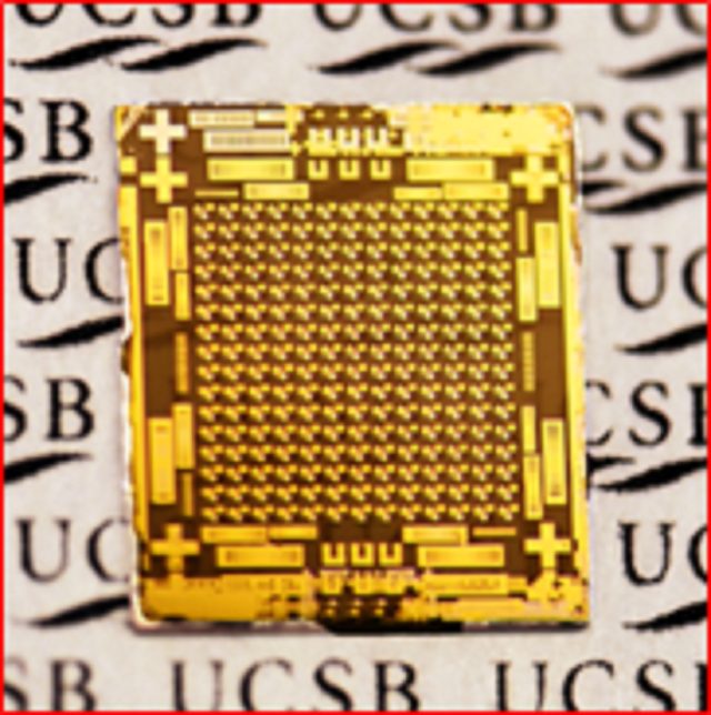
Compute-in-memory — where data processing and storage occur in the same location — is an alternative to the von Neumann architecture where data are transferred between separate memory and processing elements. The approach is expected to provide area and energy savings in data-intensive applications, and typically uses a crossbar array layout of resistive random-access memory (or memristor)-type devices. However, each memory device requires a control transistor in what is commonly referred to
as a one-transistor one-resistor (1T1R) cell format. This ensures the memory devices work reliably and efficiently, but increases the device count and circuit area. Kaustav Banerjee and colleagues have now developed a way to merge the control transistor and the memory device to create what they term a combined 0.5T0.5R memory cell. The researchers — who are based at the University of California at Santa Barbara and Xi’an Jiaotong University — create a single heterostructured device using only van der Waals materials, with graphene as the contact, tungsten diselenide as the semiconductor channel and hexagonal boron nitride as the non-volatile resistive switching element. The geometry of the contact at the graphene and hexagonal born nitride interface is optimized to confine the electric field and enhance the switching performance of the device. The devices are smaller than most 1T1R systems that use similar materials, and they exhibit switching times of around 10 nanoseconds and energies below 0.1 picojoules per bit. The memory devices can also display synaptic-like behaviour, making them potentially useful for neuromorphic applications.