NRL Research Vision & Areas
NRL is focused on innovating nanoscale devices uniquely enabled by engineering of emerging electronic, photonic and magnetic materials for a wide range of applications – from computing and sensing, to energy conversion and communication. Our overarching research philosophy is to address major challenges in these domains by pioneering fundamentally new concepts and prototypes to enable a smarter life. We employ a distinctive “atoms to applications” approach - traversing low-dimensional materials physics, predictive ab-initio modeling, electrical/thermal transport theory, and synthesis/manipulation of nanomaterials to semiconductor device design, nanofabrication and characterization as well as circuit design.
Several NRL innovations have found wide-scale implementation in the semiconductor industry or have been successfully transitioned to industry for further R&D. NRL research has made significant impact in the following areas:
We employ a distinctive “atoms to applications” approach...
Kaustav Banerjee
NRL Director and Principal Investigator
Areas


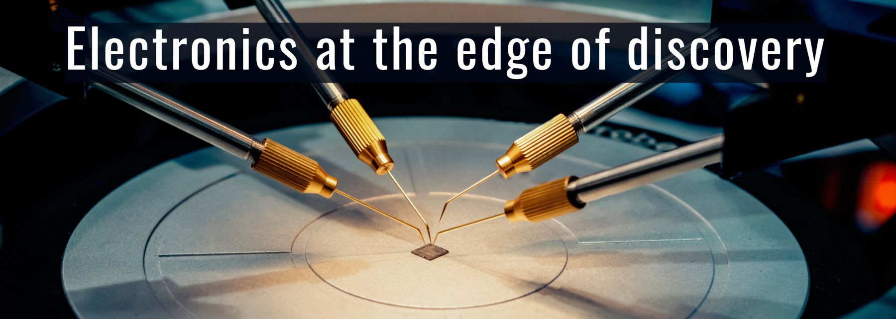
Facilities
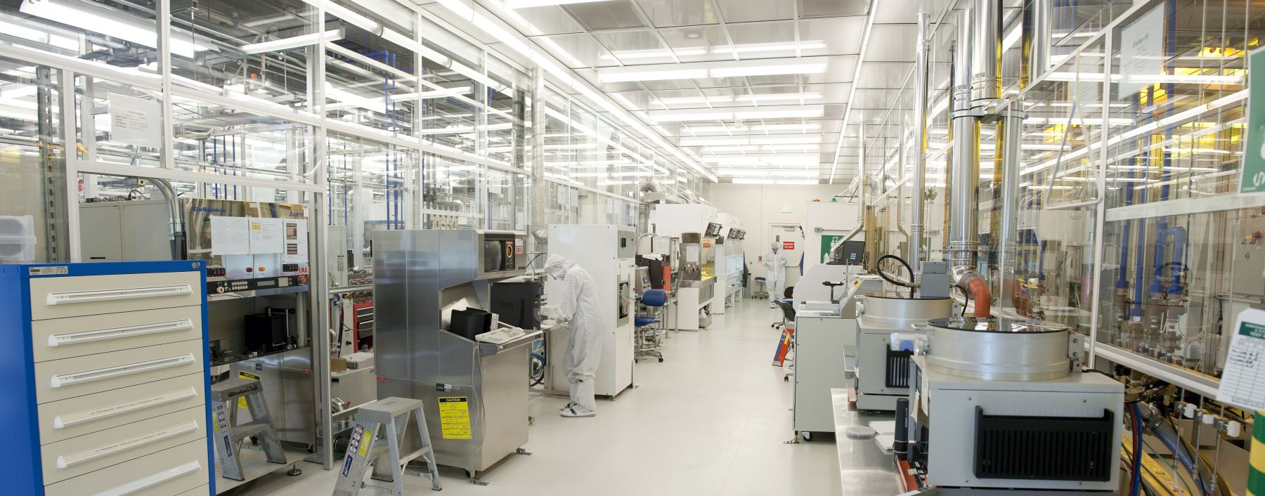
In addition to its dedicated material synthesis and characterization, simulation, and device measurement facilities, NRL has access to state-of-the-art equipment across the UCSB Nanofabrication Facility, Nanostructures Cleanroom Facility, and the Materials Research Laboratory. This makes NRL one of the most advanced research labs specializing in quantum engineered materials and devices - if we can't make it, no one can!